Address:
Plot No. B-6/5, Site 5 Surajpur Industrial Area, Block F, Surajpur Site V, Greater Noida, Uttar Pradesh 201306
For Business: +91 9212314779
For Careers: +91 84483 40400
Landline: 0120-4298000
Address:
Plot No. B-6/5, Site 5 Surajpur Industrial Area, Block F, Surajpur Site V, Greater Noida, Uttar Pradesh 201306
For Business: +91 9212314779
For Careers: +91 84483 40400
Landline: 0120-4298000

Why Simplifying PCB Design Matters?
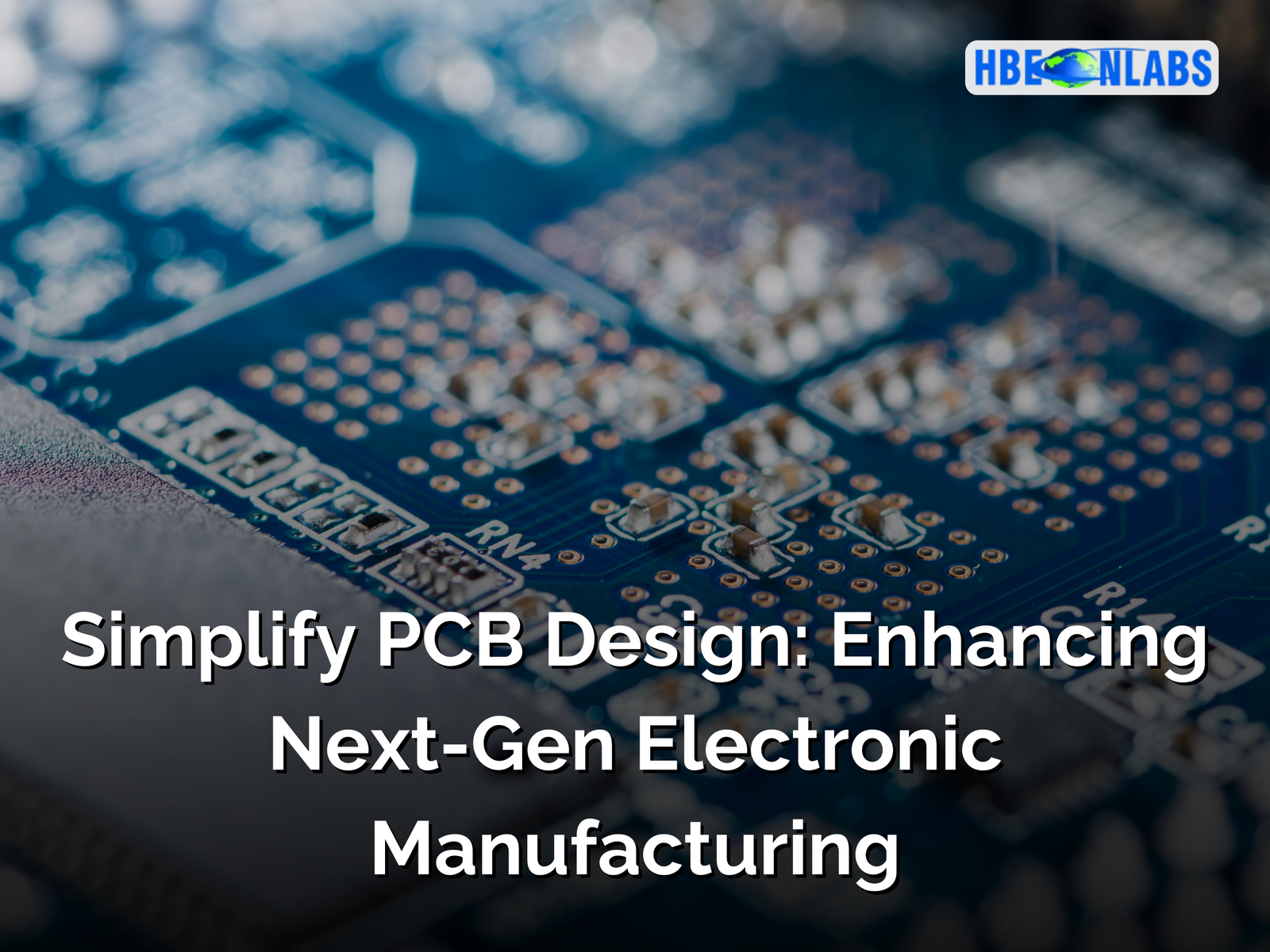
Every electronic device, from smartphones to medical equipment, relies on a Printed Circuit Board (PCB) at its core. It’s like the nervous system of any electronic product, connecting all the essential components to make the device functional.
But here’s the catch: PCB design isn’t just about connecting circuits. It’s about simplifying the design without compromising performance or reliability.
In modern electronic manufacturing services, simplifying PCB design has become a critical step. It reduces errors, lowers production costs, and ensures faster assembly processes.
Let’s take a closer look at how Simplify PCB Design is shaping the future of electronic product development and why it’s a complete changer for next-gen electronics.
Understanding PCB Design and Its Role in Electronics Manufacturing
At its simplest, a PCB is a board that holds electronic components together using conductive pathways. But not all PCBs are created equal.
Traditional PCB Design vs. Simplified PCB Design:
Example: Imagine designing a PCB for a wearable fitness tracker. A traditional design might involve excessive layers and unnecessary connections, increasing cost and reducing efficiency. Simplifying the PCB would focus on reducing these redundancies while maintaining performance.
Every unnecessary connection in a PCB design is a potential point of failure. Simplify it, and reliability improves.
Why Simplify PCB Design is Critical in Next-Gen Electronics
In electronics manufacturing, complexity doesn’t always mean better—it often means costly mistakes. Let’s get to know it better!
1. Cost Efficiency:
Simplified PCBs reduce material usage, manufacturing time, and rework costs.
Example: In mass production, even a slight reduction in PCB complexity can save thousands of dollars.
2. Improved Reliability:
Fewer connections and simplified routing mean fewer points of failure.
3. Faster Prototyping:
Simpler designs accelerate the prototyping phase, enabling quicker iterations and market launches.
4. Scalability:
Simplified PCBs are easier to scale from prototypes to mass production without introducing errors.
How Simplify PCB Design Integrates with Electronic Manufacturing Services (EMS)
Electronic manufacturing services (EMS) involve designing, producing, testing, and delivering electronic products. PCB design is one of the most crucial elements of this cycle.
The Key Connection:
Example: A leading EMS provider redesigned a complex industrial control PCB, reducing unnecessary layers and optimizing routing. The result? A 25% drop in manufacturing costs and a 30% increase in production speed.
Key Strategies to Simplify PCB Design
“A simple layout today saves hours of troubleshooting tomorrow.”
Real-Life Example: PCB Design in Consumer Electronics
Take a smart thermostat as an example. Early versions had bulky PCBs with unnecessary routing and overlapping layers, leading to manufacturing defects and increased costs.
When the PCB design was simplified:
This shows how effective Simplify PCB Design can directly impact both manufacturing efficiency and product reliability.
Note: When PCB design gets simpler, everything else gets faster, cheaper, and better.
Challenges in Simplifying PCB Design
While simplifying PCB designs brings many benefits, it’s not without challenges:
Addressing these requires expertise, experience, and close collaboration between design and manufacturing teams.
Simple Doesn’t Mean Easy
In electronic product development, the path to simplicity is often complex. But the results speak for themselves—lower costs, faster production, and more reliable products.
For manufacturers and product developers, adopting Simplify PCB Design isn’t just a technical choice; it’s a strategic one.
At HBeonLabs, we focus on designs that don’t just work but work efficiently.
If you’re looking to bring your product to life with optimized PCB designs, let’s connect and simplify together!
Partner with HBeonLabs for expert PCB design and smart electronic manufacturing services. Your idea deserves precision, simplicity, and reliability. Contact us today!